Training Course on Low-Power VLSI Design
Training Course on Low-Power VLSI Design offers a comprehensive exploration of state-of-the-art techniques and methodologies for designing energy-efficient Very Large Scale Integration (VLSI) circuits.
Course Overview
Training Course on Low-Power VLSI Design
Introduction
The pervasive demand for longer battery life, reduced heat dissipation, and sustainable electronic systems has made Low-Power VLSI Design a critical imperative in the semiconductor industry. From portable consumer electronics to IoT devices and high-performance computing (HPC), minimizing power consumption without sacrificing performance is a fundamental design challenge. Training Course on Low-Power VLSI Design offers a comprehensive exploration of state-of-the-art techniques and methodologies for designing energy-efficient Very Large Scale Integration (VLSI) circuits. Participants will delve into the intricacies of power dissipation mechanisms, architectural-level power optimization, circuit-level power reduction, and advanced power management strategies, equipping them with the expertise to create innovative, power-optimized silicon solutions.
This program provides a practical, hands-on approach to low-power VLSI design, emphasizing the application of theoretical concepts to real-world design flows. Key areas of focus include dynamic power management, leakage power reduction, voltage and frequency scaling (DVFS), and the utilization of power-aware EDA tools. Through industry best practices and case studies spanning diverse application domains like wearable technology and edge AI accelerators, attendees will learn to identify and mitigate power bottlenecks, significantly extending product lifespan, reducing operational costs, and contributing to greener electronics. The course will empower participants to become leaders in the design of next-generation, energy-efficient integrated circuits.
Course duration
10 Days
Course Objectives
- Master Power Dissipation Mechanisms.
- Apply Architectural-Level Power Optimizations.
- Implement Circuit-Level Power Reduction.
- Utilize Dynamic Voltage and Frequency Scaling (DVFS.
- Design for Leakage Power Reduction.
- Integrate Power Gating Architectures.
- Optimize Clock Gating Strategies.
- Leverage Power-Aware EDA Tools.
- Analyze Power in Memory Architectures.
- Design for Low-Power Digital Signal Processing (DSP.
- Evaluate Power for IoT & Edge Devices.
- Explore Near-Threshold Computing (NTC.
- Anticipate Future Low-Power Trends.
Organizational Benefits
- Extended Product Battery Life.
- Reduced System Operating Costs.
- Decreased Heat Dissipation.
- Smaller Form Factors.
- Enhanced Product Reliability.
- Competitive Edge in Green Electronics.
- Faster Time-to-Market.
- Improved Manufacturing Yields.
- Strategic Innovation Capability.
- Attraction and Retention of Top Talent.
Target Participants
- Digital VLSI Designers
- Analog/Mixed-Signal Designers (with an interest in power management)
- SoC Architects
- Verification Engineers
- CAD/EDA Tool Developers
- Firmware Engineers (interacting with power modes)
- Project Managers overseeing IC development
- Researchers and Academics in microelectronics
Course Outline
Module 1: Fundamentals of Power Dissipation in CMOS Circuits
- Sources of Power Dissipation: Dynamic, Static (Leakage), and Short-Circuit Power.
- CMOS Inverter Power Characteristics.
- Factors Influencing Power Consumption: Voltage, Frequency, Capacitance, and Activity Factor.
- Power Metrics: Average Power, Peak Power, Energy, and Power Density.
- Case Study: Analyzing Power Breakdown in a Simple Microcontroller Core.
Module 2: Architectural-Level Power Optimization
- Voltage Scaling and Threshold Voltage Scaling.
- Pipelining and Parallelism for Performance and Power Tradeoffs.
- Data Representation and Algorithm Optimization for Low Power.
- Voltage Islands and Multi-Voltage Design Architectures.
- Case Study: Power Optimization Strategies for a Multi-Core Processor Architecture.
Module 3: Circuit-Level Power Reduction Techniques
- Transistor Sizing and Gate Sizing for Power Optimization.
- Input Vector Control (IVC) for Leakage Reduction.
- Logic Restructuring and Resynthesis for Lower Capacitance.
- Adiabatic Logic and Energy Recovery Techniques (Overview).
- Case Study: Optimizing a Critical Path in a Digital Circuit for Minimal Power.
Module 4: Dynamic Voltage and Frequency Scaling (DVFS)
- Principles of DVFS and its Impact on Performance and Power.
- Adaptive Voltage Scaling (AVS) and Adaptive Frequency Scaling (AFS).
- DVFS Implementation Challenges: PLL/DLL Lock Times and Stability.
- Software and Hardware Control of DVFS.
- Case Study: Designing a DVFS Controller for a Mobile Application Processor.
Module 5: Clock Gating Techniques
- Importance of Clock Power in Digital Designs.
- Coarse-Grained Clock Gating: Block-Level Power Reduction.
- Fine-Grained Clock Gating: Register and Gate-Level Power Optimization.
- Clock Gating Synthesis and Verification Challenges.
- Case Study: Implementing Effective Clock Gating in a Digital Signal Processing (DSP) Block.
Module 6: Power Gating Methodologies
- Principles of Power Gating: Minimizing Leakage Power in Idle Modes.
- Header and Footer Switches: Sizing and Placement.
- Retention Mechanisms: State Retention Flip-Flops (SRFFs) and Retention Latches.
- Power Gating Control and Sequencing.
- Case Study: Designing a Power-Gated Peripheral Block for an IoT Device.
Module 7: Low-Power Memory Design
- SRAM Cell Design for Leakage Reduction and Read/Write Stability.
- DRAM Power Saving Modes: Self-Refresh, Power Down.
- Non-Volatile Memory (NVM) Power Considerations.
- Cache Design and Power Management.
- Case Study: Analyzing Power Consumption of Different Memory Hierarchies in an SoC.
Module 8: Power Estimation and Analysis
- Gate-Level Power Estimation: Activity Factors and Switching Probability.
- RTL-Level Power Estimation: Architectural Models.
- System-Level Power Modeling: Transaction-Level Power Analysis.
- Power-Aware Simulation and Verification.
- Case Study: Performing Power Analysis on a RISC-V Microprocessor Core using EDA Tools.
Module 9: Power Management Unit (PMU) Design
- Role of the PMU in System-on-Chip (SoC) Power Management.
- Voltage Regulators: LDOs and Switching Converters.
- Power Domains and Isolation Cells.
- PMU Communication Interfaces (e.g., PMBus).
- Case Study: Architecting a PMU for a Complex Heterogeneous SoC.
Module 10: Low-Power Analog and Mixed-Signal Design
- Power Considerations in Analog Blocks: ADCs, DACs, PLLs.
- Low-Power Amplifier and Filter Design.
- Power Management for Sensors and RF Transceivers.
- Voltage and Current Reference Design.
- Case Study: Designing a Low-Power Analog Front-End for a Biomedical Sensor.
Module 11: Low-Power Design for IoT and Edge Devices
- Energy Harvesting and Scavenging Techniques.
- Ultra-Low Power Radios and Communication Protocols.
- Always-On Domains and Event-Driven Architectures.
- Tradeoffs between Performance, Power, and Cost for Edge AI.
- Case Study: Power Budgeting and Optimization for a Smart Wearable Device.
Module 12: Advanced Power Optimization Techniques
- Body Biasing: Forward and Reverse Body Biasing.
- Sub-Threshold and Near-Threshold Computing: Challenges and Opportunities.
- Approximate Computing for Energy Efficiency.
- In-Memory Computing and Processing-in-Memory (PIM).
- Case Study: Exploring the Energy Benefits of Near-Threshold Operation for Specialized Processors.
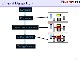
Module 13: Power-Aware Physical Design
- Power Grid Design and IR Drop Analysis.
- Electromigration (EM) and Self-Heating Considerations.
- Placement and Routing for Power Minimization.
- Decoupling Capacitor Placement and Sizing.
- Case Study: Optimizing the Power Delivery Network of a High-Performance Digital Block.
Module 14: Verification of Low-Power Designs
- Power Intent Specification: UPF (Unified Power Format) and CPF (Common Power Format).
- Formal Verification for Power Gating and Isolation.
- Low-Power Test Patterns and Design for Testability (DFT) for Power.
- Power-Aware Functional Verification.
- Case Study: Verifying a Multi-Power Domain Design using UPF.
Module 15: Future Trends and Research in Low-Power VLSI
- Neuromorphic Computing and Spiking Neural Networks for Ultra-Low Power AI.
- Quantum Computing Power Implications.
- Advanced Materials for Low-Power Devices (e.g., 2D Materials, Ferroelectrics).
- Design Methodologies for Extreme Energy Efficiency.
- Case Study: Discussion on the Power Challenges and Opportunities in Beyond-CMOS Technologies.
Training Methodology
This course employs a participatory and hands-on approach to ensure practical learning, including:
- Interactive lectures and presentations.
- Group discussions and brainstorming sessions.
- Hands-on exercises using real-world datasets.
- Role-playing and scenario-based simulations.
- Analysis of case studies to bridge theory and practice.
- Peer-to-peer learning and networking.
- Expert-led Q&A sessions.
- Continuous feedback and personalized guidance.
Register as a group from 3 participants for a Discount
Send us an email: info@datastatresearch.org or call +254724527104
Certification
Upon successful completion of this training, participants will be issued with a globally- recognized certificate.
Tailor-Made Course
We also offer tailor-made courses based on your needs.
Key Notes
a. The participant must be conversant with English.
b. Upon completion of training the participant will be issued with an Authorized Training Certificate
c. Course duration is flexible and the contents can be modified to fit any number of days.
d. The course fee includes facilitation training materials, 2 coffee breaks, buffet lunch and A Certificate upon successful completion of Training.
e. One-year post-training support Consultation and Coaching provided after the course.
f. Payment should be done at least a week before commence of the training, to DATASTAT CONSULTANCY LTD account, as indicated in the invoice so as to enable us prepare better for you.